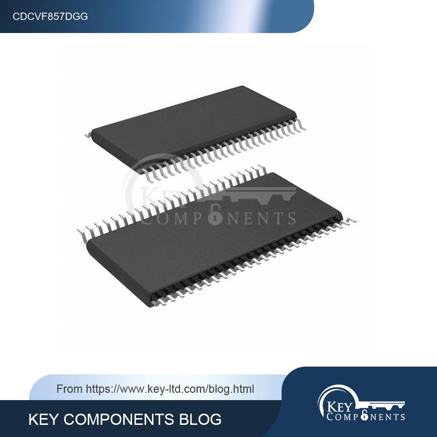
It is a 48-TSSOP surface mount package that can operate at a maximum frequency of 220 MHz. The device is an ideal choice for applications that require precision frequency and phase synchronization between different electronic circuits. In this article, we will discuss the key features and specifications of CDCVF857DGG and explore its potential applications in various electronic devices.
Paragraph 1: Introduction to CDCVF857DGG CDCVF857DGG is a highly-integrated PLL clock driver that can generate precise clock signals with low noise and jitter. The device is compatible with SSTL-2 input and output interfaces, and it supports a 2:11 input-to-output ratio, which makes it suitable for high-speed data transfer applications. Additionally, CDCVF857DGG features a bypass mode that can disable the PLL function and provide a direct clock output to the system.
Paragraph 2: Key Features of CDCVF857DGG CDCVF857DGG has several key features that make it an ideal choice for high-frequency applications. Firstly, the device has a wide input voltage range of 2.3V to 2.7V, which makes it compatible with a variety of power supply options. Secondly, the device has an operating temperature range of -40°C to 85°C, which ensures reliable performance under extreme environmental conditions. Lastly, CDCVF857DGG has differential input and output interfaces that eliminate common-mode noise and provide a robust interface between different electronic circuits.
Paragraph 3: Applications of CDCVF857DGG CDCVF857DGG can be used in a variety of electronic devices that require precise timing and frequency synchronization. Some of the potential applications of CDCVF857DGG include high-speed data transfer systems, wireless communication systems, networking equipment, and digital signal processing systems. For example, in a high-speed data transfer system, CDCVF857DGG can be used to generate clock signals for data converters, serializers/deserializers, and other high-speed interface modules.
Paragraph 4: Benefits of CDCVF857DGG CDCVF857DGG provides several benefits over traditional PLL clock drivers. Firstly, the device has a low jitter and phase noise, which ensures accurate timing and synchronization between different electronic circuits. Secondly, the device has a fast lock time and a high frequency range, which makes it suitable for high-speed data transfer applications. Lastly, CDCVF857DGG is a highly-integrated device that requires minimal external components, which reduces the overall system cost and complexity.
Paragraph 5: Conclusion In conclusion, CDCVF857DGG is an active PLL clock driver that offers high performance, reliability, and versatility. The device is ideal for high-frequency applications that require precise timing and synchronization between different electronic circuits. With its wide input voltage range, differential input/output interfaces, and bypass mode, CDCVF857DGG can be used in a variety of electronic devices and systems. Whether it is used in wireless communication systems, networking equipment, or digital signal processing systems, CDCVF857DGG can provide accurate and reliable clock signals for high-speed data transfer and processing.